Saturday, May 29, 2021

Agilent 3458a in the lab

This is the second 8.5 digits DMM in my lab and I'm very excited to own it!

This post includes the following topics:

- Modifications : the new temperature set point for the voltage reference for increasing long term stability and the fan noise reduction. 

- Maintenance : Replacing batteries for calibration SRAM and the fan filter.

- Testing some DMM's parameters : noise, leakage current, 1 day and 90 days stability, CAL? 72, and INL against programmable Josephson voltage standard.

- Some useful subroutines loaded with the AR-488 GPIB adapter.


Modifications

The default temperature set point for LTZ1000A Voltage reference was reduced with soldering 100K resistor in parallel to the 15K resistor. This modification improve the long-term stability of the voltage reference. I followed the instructions from Dr. Frank and Illya Tsemenko from xDevs.com. The used resistor model is RNC90Z from Alpha Electronics/VishayPG with max 2ppm/°C TCR. 

WARNING : This modification will require a fresh new adjustments of your DMM and will need time the new zener voltage to be stabilized. 


The resistor was placed in the X411 component designator. The soldered vias were un-soldered with the help of needle and solder iron. 


The measured equivalent resistance was near to 13K which match with the LTZ1000(A) datasheet value.  


The next modification I made was the fan noise reduction. When the DMM is stored in a rack located in industrial/metrology laboratory, this is not a big problem, but at home the fan noise is very annoying. 

The selected fan for replacement was Noctua NF-A6x25 FLX with 2 adapters for reducing the fan speed to 2400 and 1600 rpm. Those adapters are actually just resistors to lower the input voltage. Because the fan voltage of the 3458a is 15V, these adapters are very handy to ensure that the fan voltage does not exceed the 13.2V limit of the Noctua fan.

In result, the noise was reduced significantly and actually is much silent from my second 8.5 digits DMM - Advantest R6581T. There is still noise, but in very acceptable levels.

After replacing the fan, the internal temperature increased with 4°C : the differences  between the ambient and internal temperature was 12°C with the old and 16°C with the new fan. 

Maintenance

The batteries which keeps the calibration constants in the RAM were replaced. Very comprehensive information about the replacement process can be found in the Martin Lorton's video.


The closest to the original fan filter which I was able to found was the 30 PPI polyurethane foam filter made by company named Multicomp Pro. The part number is MC32657 and can be purchased from Farnell.

You can see in the picture the original filter in the left and the replacement in the right:


Testing some DMM parameters

Noise

The noise measurements were performed with a short PCB across input binding posts and enabled the "Auto Zero" option. The "Digits" column calculates effective number of digits based on standard deviation results for 68% probability. The "RMS noise limit, uV" column data are calculated according the "Additional Errors" and "*RMS noise " tables in the 3458a datasheet. 
The time for measurement was 200 seconds for every range and NPLC.
The 0.1/1/10V ranges for 1 and 100 NPLC were in the spec, but out of the spec for 10 NPLC with around 0.02 ppm.

Range, VNPLCSamplesSTDEV/RMS noise, uVRMS noise limit, uVDigits
10100500.0810.18.17
1100500.0210.027.76
0.1100500.0190.026.80
10105000.2690.257.65
1105000.0660.057.26
0.1105000.0740.056.21
10150000.54117.35
1150000.1370.26.94
0.1150000.1110.26.03


Leakage current

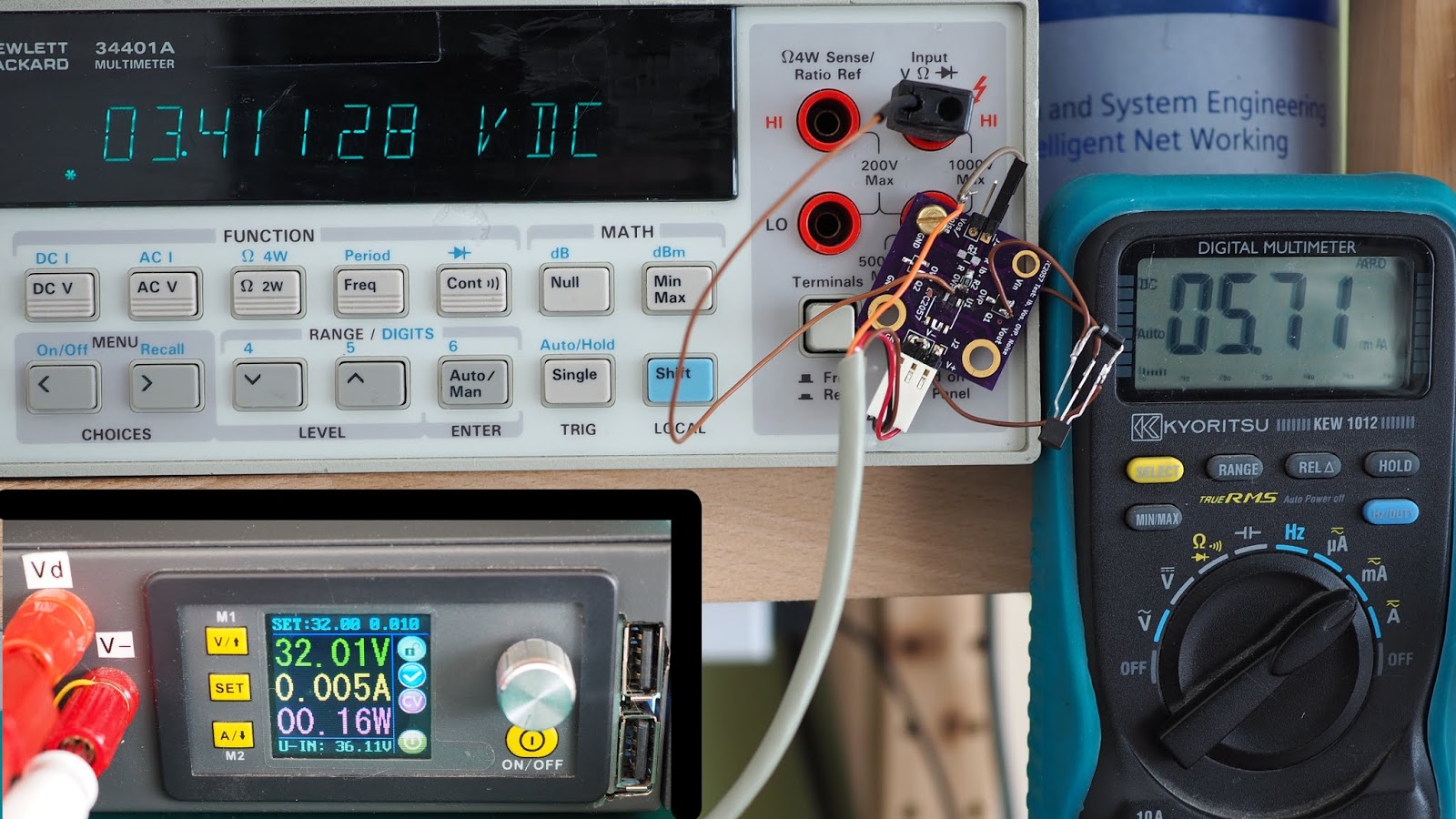
The leakage test was performed with 1 and 10 MOhms resistors attached to the binding posts. The measured generated voltage was converted to the leakage current. All measurements are within the 20pA limit at 25°C.

R inputRangeLeakage, pA
1 MOhms10 V1.66
1 MOhms1 V0.75
1 MOhms0.1 V1.7
10 MOhms10 V0.74
10 MOhms1 V2.33
10 MOhms0.1 V1.7

One day stability

In period of 10 days, I measured the LTZ1000 zener output voltage after performing ACAL. I choose the zener output (7.15V) instead the 10V because it should be more thermal stable. The difference between current day and previous day was recorded and shown in the following chart. The 24 hour spec limit for accuracy in the 10V range is 0.5ppm from the reading and 0.05ppm from the range. For the 7.15V zener output this is ~0.4ppm. For two consecutive days, this limit was exceeded with less than 0.15ppm. The recorded ambient and DMM internal  temperature peak to peak value was ~2.67°C and standard deviation was ~0.8°C.

90 days stability

In period of 93 days with 3 week interruption, the 10V output from the voltage reference was recorded and the stability was better than +/- 1ppm which is in the spec limit of the 3458A 90 days relative accuracy:  4.15ppm for 10V. During this period, the recorded ambient and DMM internal  temperature peak to peak value was ~5.55°C and standard deviation was ~1.21°C.

CAL? 72 calibration constant test

According service note SN18A from Keysight, the DMM can have short term drift more than 0.43ppm daily. To verify this issue, at least 7 days data should be recorded. I decided to record this constant during the 90 days stability test and here are results. The short-term drift value calculated by the formula given in the service note SN18A was less than 0.02ppm peak to peak, standard deviation 0.005ppm. At the end of the period, the last value of the C variable was 0.005ppm. Far less than the stated 0.43ppm value. I recorded also the day to day drift and the peak to peak value was 0.687ppm, standard deviation 0.162. 


Integral nonlinearity measurement against programmable Josephson voltage standard

This is may be the most important parameter when you use a DMM in the metrological field. When you make ratio transfer measurements from one calibrated standard to other one, you want to have the minimum INL. This will minimize your uncertainty budget.

The INL test was performed in the Bulgarian Metrology Institute using their new Josephson programmable voltage standard manufactured by Supracon.


Based on data from the protocol, I made charts against the linearity specification found in the 3458a datasheet. The linearity is within the specified limits, except the 0.1V range.


Using 3458a with GPIB controller

Unfortunately, the 3458a DMM is not very user friendly when it is used from the front panel. It is far away from the Advantest R6581T user interface which can be used almost without reading the documentation available in Japan language only :-) . The only way to get desire functionality during measurements is to write BASIC subroutines.  To load them, you need a GPIB controller.
Last year I made AR488 based GPIB controller which was used to communicate with Advantest R6581T and HP 34401A multimeters. It is enough reliable if you set the BOD voltage to 4.3 for the atmega32u4 microcontroller. The default one is set to 2.6V which cause very often firmware corruption due voltage glitches.


Using Serial/UART port terminal program (like CuteCom under GNU/Linux OS) you have to write only the following commands to enter into the remote mode:

++ren 1
++addr GPIB_ADDRESS
++auto 1
ID?

Where GPIB_ADDRESS is DMM GPIB address set with ADDRESS XX command from the front pannel.

When you upload the subroutines from a file, set value 100ms in the "Char delay" field to avoid errors during transmission.

I made two basic subroutines one of the which makes the real measurements and the second one (STAT_INFO) which display on the DMM's display, the statistical results after the measurements. The result contains number of samples, standard deviation, peak to peak, average, minimum and maximum values. Once the subroutines are loaded into the DMM, they can be invoked with the "CALL SUB_NAME" command. It is very convenient to store "CALL" command in one of the DefKey for fast access to all of your subroutines.  

SUB STAT_INFO
REAL MINV, MAXV, MEANV, STDEVV, P2PV, NUMV
RMATHV LOWER, MINV
RMATHV UPPER, MAXV
RMATHV MEAN, MEANV
RMATHV SDEV, STDEVV
RMATHV NSAMP, NUMV
LET P2PV = MAXV-MINV
DSP "N=" NUMV " STDEV=" STDEVV " P2P=" P2PV " AV=" MEANV " MIN=" MINV " MAX=" MAXV
SUBEND

SUB DCV_XXXXXX
PRESET NORM 
MEM FIFO 
TRIG HOLD 
MFORMAT DINT  // Store the result in 4 bytes
DCV 10                 // Change here the DCV range
NRDGS 15            // Change here the number of samples
NDIG 8 
NPLC 100
AZERO ON
DISP MSG 
TRIG SGL 
MMATH STAT 
BEEP 
WAIT 500
BEEP 
WAIT 500
BEEP 
WAIT 500
BEEP 
WAIT 500
BEEP 
TRIG AUTO
DISP ON
SUBEND 


Saturday, April 10, 2021

The first PCB design of the open source voltmeter is ready

After 5 years of researching, developing and testing, I'm ready with the first PCB design:


The main PCB fits in 10x10cm layout and contains 4 modules : Analog front-end with OVP and two voltage ranges, ADC based on LTC2440, Voltage Reference based on LTC6655 and power supply using classic LM317/LM337 LDO. 
The PCB does not includes the controller for reading out and displaying the measurement results from the ADC.

I have to double check availability of the components, schematics and layout for possible errors before ordering all PCBs next week.

Analog front end schematics:


ADC schematics:


Power supply and voltage references schematics:


There are 2 more PCB : 
- one for AC input circuit with over-voltage protection using GDT and varistors (based on IEC 60950-1 schematics)  ̶a̶n̶d̶ ̶p̶r̶o̶t̶e̶c̶t̶i̶o̶n̶ ̶a̶g̶a̶i̶n̶s̶t̶ ̶i̶n̶t̶e̶r̶f̶e̶r̶e̶n̶c̶e̶ ̶v̶o̶l̶t̶a̶g̶e̶ ̶f̶r̶o̶m̶ ̶t̶h̶e̶ ̶m̶a̶i̶n̶s̶. A friend of mine gave me advice, that main filter is not needed when transformer is used, because it acts like low pass filter for external interference. Only if switching power supplies are used, it is worth to place such of filter. A reader of the blog notice that the transformer is not ideal and always a capacitance exists between the primary and secondary side. Which means that any AC signal (noise) can pass through the transformer. The frequency band is limited to the capacity value and the transformer's frequency loss. So far I was not able to find a tests results about this impact. I found an application note from Schaffner where noise filter is placed between a main line and linear power supply. 
- one for AC-DC conversion which includes again over-voltage protection using TVS diodes and CLC ripple filter. 
I paid special attention for input over-voltage protection after 2 times literally burning the op-amp in my LTZ1000 based 10V voltage reference due mains AC over-voltages. 

Here is the AC input PCB:


Here is the AC-DC PCB:

The AC-DC PCB supports 2 sizes of transformers.

Based on LTSpice simulation and LM317/337 ripple rejection vs. output load current chart, I expect to have around 15uV noise in the 0.1-0.3A current load range after LDO outputs.

And one more news : finally I bought an Agilent 3458A DMM :-)


The DMM is 10 years old and I will make later a post about the modifications and testing some DMM parameters, I was able to made. This will include also a INL against Programmable Josephson voltage standard. 
I think to make a voltage calibrator based on AD5791 DAC and with the help of the 3458a linearity I can measure the real INL of the AD5791. Once this is done, I will be able to measure the INL of the open DCM voltmeter using the AD5791 based calibrator. 


Sunday, December 27, 2020

Temperature coefficient and the humidity effect on the LTC6655 voltage output

Between the 11 April and 14 May 2020 I tried to measure the 1 month stability of the LTC6655. During this period I made 80 measurements and the result is shown in the following chart:


StatRH %Tamb °CV ref, V
Min2419.82.5003369
Max5426.62.5003616
Peak to Peak306.80.0000247
ppm0.33ppm/%RH1.45ppm/°C9.88ppm

Based on the statistic data, the temperature coefficient was 1.45 ppm/°C and the dependency from humidity was 0.33ppm/%RH. The TC for LTC6655B was below the 2ppm/°C. There is no explicitly given value for the humidity's effect on the voltage output, but was mention that "... humidity sensitivity can be reduced to less than 35ppm for a change in relative humidity of approximately 60%." if PCB slots cuts are made around the LTC6655. This is equal to 0.58ppm/%RH. Because I used small MS8 adapter, I thought that the measured value corresponds to the datasheet value.

However, looking into the chart it is visible that the output voltage is affected more by humidity than by temperature. So I tried to extract measurement data, where the fluctuation of the temperature is relative small and got the next chart, where the dependency is more clear:

According the datasheet, only the LS8 package is not affected by the humidity. I have one LS8, but I do not have PCB to solder on it. So the only option to see what is the real temperature coefficient is to insulate with Fibran XPS the box where the LTC6655 is placed and to fill it with several silica gel packages. This would allow me to keep the humidity in very narrow range.


For period of 12 hours, I was able to keep the relative humidity inside the box in the range of 0.9%, while the external humidity was in the range of 6.87%. The relative humidity and temperature measurements were performed with pair of BME 280 sensors. The result of the measurements are shown in the chart below. It is clearly shows now that the dependency between the temperature in the box and the voltage output is linear. The measured voltage deviation was 5.32ppm for 2.8 °C difference, which makes 1.9ppm/°C within the datasheet specification. 


I wanted to make the same experiment for longer period of time, so the silica gel bags were baked into the oven for about 3 hours in 100°C. In the next 6 days, after 23 measurements, the humidity in the box was changed with 4.3% RH (0.72% per 24h) which is about 3 times better compared to the previous time. The temperature coefficient was not changed so much from the previous time: 1.89ppm/°C for 4.36°C temperature range.


Here an idea popped into my head : if this linearity can be proved for the +/- 5°C and there is no hysteresis within this interval, it would be possible to characterize the LTC6655 for this range and to use the data for an artificial calibration like the HP 3458a and the Advantest R6581 multi-meters. But for that, I have to make PCB for the LS8 package and to make temperature controlled camera.


Friday, December 25, 2020

Revised analog front-end : Replacing the analog switch, part 4/4

In the post for the automatic voltage range, I used the analog switch ADG5419 to switch between the low and the high voltage ranges. I was wondering if the switch can be replaced with the shutdown feature of the LTC2057 op-amp. According the datasheet when the LTC2057 is in the shutdown mode : "... the output presents a high impedance to external circuitry". If the outputs of the op-amps are shorted and the SD inputs are feed with opposite signals for each op-amp, in theory this is equivalent to a SPDT switch. The switch is not expensive one (it cost around 5USD), but the maximum voltage which can stand (+/- 22V) was less than the voltage which I will use for the LTC2057HV. So usage of the ADG5419 cost me 2 more power rails which I want to avoid.


Тhis raised the following question : what kind of glue logic ("A" in the schematics above) I have to put between the outputs of the MAX990  comparators and the SD/SDCOM op-amp inputs? 

The output pin of the MAX990 is an open drain and a pull-up resistor to the positive rail have to be added. The voltage outputs of the MAX990 are between -2.5V+Vds(of the open-drain stage) when input voltage is above 2.048V and +2.5V when input voltage is below 2.048V.

From the LTC2057 datasheet we have the following information: "Shutdown control is accomplished through differential signaling. This method allows for low voltage digital control logic to operate independently of the amplifier’s high voltage supply rails.". And the tables with the logic and operating voltage ranges:

From the operating voltage range we had the restriction that voltage between the SD and SDCOM must be no more than 5.4V and it should be between the op-amp's power rails (except for the SDCOM max value). This was fine as far as the MAX990 outputs are between -2.5V and +2.5V. If the SDCOM is connected to the -2.5V power rail, I need two opposite signals from the MAX990 outputs which to be connected to the SD pins. 

I thought : why not to put an NOR gate 74x logic? The negative input voltage is not a problem if the Vss is connected to the -2.5V power rail and the Vcc is connected to the +2.5V. So, I made a breadboard proof of concept and putting the scope probe on the shorted outputs of the LTC2057 op-amps, I got a very clean, 2 us transition time between the two input signals.


Sunday, April 26, 2020

Revised analog front-end : Over Voltage Protection, part 3/4

This post will focus on a practical selection of over-voltage protection components, their parameters, schematics and needed calculations. The tests' results are given at the end.

The standard over-voltage protection in the 3-4 digits handheld digital multimeters is build with a current limiting PTC, placed in series and voltage spike suppressor MOV, which is placed in parallel to the input buffer. When we are talking about 6+ digits DMM, this solution is not suitable due to the high current leakage of the PTC and the high resistance, current leakage and capacitance of the MOV.

For voltage protection up to 100V DC, ultra-low leakage diodes or JFET transistors can be used. For higher voltages, I think a Gas Discharge Tube (GDT) can be used due to their absent of the current leakage.

How over-voltage protection works


When the input voltage is greater than the positive (or less than the negative) voltage rail and the forward diode voltage, the diode will begin to conduct and the current will pass from the limiting resistor through the diode to the positive or negative power rail. The positive rail must sink the current and the negative rail must source the current.

There is one problem: when a standard LDO is used for positive rail, it can not sink a current. As a result, the current through the diode will increase the voltage on the positive rail and can damage the circuit under the protection.

There are two solutions to this problem: to use a buffer op-amp which can sink between several to tens mA or to use schematics I found during the op-amp selection from the ADA4177 datasheet - an PNP transistor which "re-routes" the current from the diode to the "sinking" ground. I tried the solution in the ADA4177 and it works perfectly.

If a dual-polarity power supply is used for the op-amp, the negative power rail will source the current through the diode and the voltage will not be increased when the input voltage exceeds the negative power rail.

The maximum input voltage is the sum of the power supply voltage and the continuous reverse voltage that can withstand the diode. The input voltage for the op-amp will be clamped to the following values:
- For the positive over-voltage: the sum of the positive power rail voltage, the diode's forward voltage and the base-emitter voltage of the PNP transistor.
- For the negative over-voltage: the sum of the positive power rail voltage and the forward voltage of the diode.

The clamping voltage must not exceed the maximum allowed power supply of the op-amp. Let's give one example with LTC2057HV that has spec of 60V supply peak to peak voltage (65V absolute maximum). If the op-amp is supplied with +/- 27V, this will give 60V-(2*27V)=6V maximum clamp above the positive or negative power rail. That means that maximum allowed value is +/-33V.

Component Selection


On the market there aren't so many diodes that have pA range leakage current. The few of them are: BAV199, BAS416 and PAD series diodes with guaranteed maximum values, but they are very expensive. The alternative is a JFET transistor like MMBF4117 with shortened drain and source pins.

Which parameters should you look at? Here is the list:

- "Reverse/leakage current" for diodes or "Gate to Source Reverse Current (IGSS)" for JFET transistors. The value should be in pA range, preferably less than 10pA.

- "Continuous reverse voltage" for diodes or "Gate to Source Breakdown Voltage (V(BR)GSS)" for JFET transistors. The value should be as high as possible.

- "Continuous forward current (IF)" for diodes or "Continuous Forward Gate Current (IFG)" for JFET transistors. This is the maximum current which has to be limited by a serial resistor.

The maximum reverse voltage that can be applied is the power supply voltage and the maximum value of the diode's continuous reverse voltage. The current which will flow through the resistor and the diode is:

I limit = (Vin - (Vsupply + Vfwd + Vpnp*))/Rlimit

Where:
- Vin is the input voltage.
- Vsupply is the voltage on the power supply rail.
- Vfwd is the forward voltage of the protection diode.
- Vpnp is the optional base-emitter voltage if positive sink schematics is used.
- Rlimit is the value of the limiting resistor.

The limit current value must not exceed the maximum value of the diode's continuous forward current and the resistor's power rating has to be selected based on the current and the resistance.

The table below shows calculated data for the dual diode BAV199, the single diode BAS416 and the JFET transistor MMBFF4117. Two values of the limiting resistors are given - 2K and 10K.

BAV199/BAS416MMBF4117BAV199/BAS416MMBF4117
V supply, V27272727
Max reverse voltage, V75407540
Max protection, V1026710267
Max current, mA160/20050160/20050
Limit resistor, Ohms200020001000010000
Limit current, mA23.56.04.71.2
Limit Resistor Power, W1.1050.0720.2210.014
Noise, RMS uV 1pA/√Hz0.010.010.030.03
Leakage voltage (100pA), uV0.200.201.001.00

Calculated values of noise and leakage voltage are shown in the last two rows in the table. 
The RMS noise value is calculated based on relative high current noise density of 1pA/√Hz. Even with 10K limiting resistor, the noise is low and can be ignored. 
However, the error due to current leakage of the whole front end which includes the reverse current of diodes and the input buffer can be significant. In the table, calculation shows that for 100pA total leakage which was my total error budget, the voltage error can be between 0.2 and 1uV respectively for 2K and 10K resistor. On the 1V range, this makes 0.2-1.0 ppm error.

The small value of the limit resistor is preferably, but this will increase the current. Maybe the 2K resistor is a good trade-off: the maximum error due to leakage  of 100pA is 0.2uV and the resistor power is around 1W for the BAV199/BAS416.

The test

The PCB made for the op-amp test from the previous post was used for the test. I soldered two JFET MMBF4117 transistors for the over-voltage protection. The limiting resistor was 5K (2x10K in parallel). For the test with the current sink, I added an external PNP transistor and a diode.

Additional circuits for the current sink.
I used two PSU:
- A small, custom made PSU which contains a Digital DC-DC Ruideng DPS 3003 with voltage range of 0-32V and two regulated LDO in the range of -/+ 1.3V to 30V. The DC-DC converter and the both LDO share same common ground.
- Analog HP 6237B PSU with dual polarity outputs +/- 23V and one single 18V output.  


Since I do not have high voltage PSU, I had to set the power supply to much lower values +/- 2V and apply up to 32V input voltage.  

Positive over-voltage test description:
- The power supply rails were set to +/- 2V using the LDOs
- The input voltage was set from 0 to 32V with 1V step using the DPS 3003
- The following voltages and current I was monitoring: the positive rail V+ (Advantest R6581T), the clamp voltage Vclamp (HP 34401A), the input current through the limiting resistor I limit (Kyoritsu KEW 1012)
- The test was made two times: once with sink current circuits and without it.


Test without the current sink circuit.


Test with the current sink circuit.
The pictures show when the current sink circuit is used, the current which flows through the diode and goes to the common ground. This is visible in the current measurement of the DPS 3003. When the current sink circuit is not used, the current is "missing" on the DPS 3003 display, but the KEW 1012 multimeter shows that it actually exists.  The test results show, that this extra current is the reason for increasing positive power rail. 

And here are results from the test:
The red solid line is voltage on the positive power rail with current sink circuit. The voltage was stable at 2V during the whole ramp-up. 
However, if we look into the blue solid line (without current sink), we can see during ramp-up of the input voltage went from 21 to 32V, the positive power supply was increased from 2V to 2.7V. The dependency is very linear and will be further increased if we continue to rump-up.
The same linear increasing of the voltage is observed for the voltage clamp when the current sink circuits is not used (the blue dash line). However, the red dash line which is the voltage clamping value with current sink circuit shows stable value across 21-32V range. 
Using linear regression, I can estimate increasing the voltage clamp up to 4V for 40V input voltage and up to 6.3V for 75V input voltage when current sink circuit is not used. This can destroy the op-amp if there is not enough head-room of the power supply.
There is no difference in the current passes through the resistor and the diode. This is visible with the blue and red dot lines. 


Negative over-voltage test description:
- The power supply rails were set up to +/- 2V using the HP 6237B PSU.
- The input voltage was set from 2 to -30V with 1V step using the negative LDO.
- The following voltages and current were monitored: the negative rail V- (Advantest R6581T), the clamp voltage Vclamp (HP 34401A), the current through the limiting resistor I limit (Kyoritsu KEW 1012).


Here the negative power rail voltage is constant during the input voltage ramp-up. The clamp voltage is also relative constant after input voltage exceeds the power rail and diode's forward voltage.

Update 15 April 2021:
I got a mail from blog's reader with a link to Maxim's Application Note 4035 about "Overvoltage protection for sensitive amplifier applications". The interesting part is "Differential Diode Protection".