Sunday, March 29, 2020

Revised analog front-end : op-amp selection and test, part 2/4

In this post I want to find out if a single buffer op-amp can replace the classic schematics used in the old days of DMM. I tested some parameters which are critical for the analog front-end. Some of them are given only as typical values and I want to know what is maximum value I can expect.

Based on the available schematics of old DMM (HP/Agilent 34401A, 34420A, 3458A, Datron 1281/1271, Keithley 2001), we can see that a pair of  JFET in common source or source follower circuit are used in front of the main buffer op-amp. This is because back then a single op-amp that can satisfy all criteria for error budget, was not available. Mainly these errors are related to input bias current and noise. For example the HP 34401 uses the OP-27GS op-amp which has very high bias current and current noise density. To solve this problem, a matched J-FET source-follower pair (NPDSU406) was used in front of the OP-27GS. This produces other problems which were resolved with additional circuits. More information can be found in the book "The Art of Electronics". I want to avoid this complexity, so I can find if newer op-amps are good enough. 

The only exception I found was the Keithley 2000 model where LTC1050C op-amp is used in bootstrap schematics. This allows the rated for maximum +/- 9V supply operation op-amp to be used for input signals up to +/- 12V (20% over range for the 10V range).


Selection of op-amps


In the previous post I made error budget for op-amp parameters and now I have to select available op-amps on the market. I made 3 groups of them : 
  • op-amps capable to handle input signals up to +/- 22V full scale range.
  • op-amps capable to handle input signals up to +/- 12V full scale range.
  • op-amps with errors below my threshold, but with maximum power supply under 10V. Using bootstrap schematics they can be used for input signals up to 22V. It's kind of a back-up plan if the previous 2 group failed.
After few weeks of looking for available op-amps and collecting parameter values, I selected 3 op-amps for the first group : LTC2057HV, ADA4522, MCP6V51 and 3 in the second group : OPA140, OPA192, LT1024A and 5 in the last group : ADA4530, ICL7652, LTC1052C, TLC2654AC, OPA376. 

Additionally I added the OP-27GS and LTC1050C as comparison to the selected op-amps.

In the tables below, the parameters are sorted by my priority given in the first column. All values which do not fit in my error budgets are colored in red.
The error budget is:

  • Ibias less then 50pA
  • Voltage noise, p2p value less than 4.4uV for the 22V range and less than 2.4uV for the 12V range. This is equivalent to 7 digits. The test for this parameter will be performed with short between positive input and the ground. 
  • Current noise density, RMS value less than 1041 fA/√Hz for 22V Range and 557 fA/√Hz for 12V Range. My criteria for this threshold is to reach a 6 digits when the input resistance is 1MOmhs and take into account the previous voltage noise thresholds.
  • Estimated Effective Number Of Digits (ENOD) for 99.7% probability. Combining voltage noise, current noise density and the input resistance must provide at least 6 digits for 12V or 22V ranges when input resistance is 1MOhms or at least 7 digits when the inputs are short. The used formula is:
        ENOD = Log10( FS/NoiseP2P)
        Where:
         - FS in Volts is the full scale for the range including the over-range. In the case of the 10V range, 12V over-range, the value is 24V and in the case of the 20V range, 22V over-range, the value is 44V.
           -  NoiseP2P in Volts is the peak to peak noise calculated by the following formula:
          NoiseP2P = 6.6 * SQRT (VnoiseRMS2+(InoiseRMS*Rin)2+RinNoiseRMS2)
          
         VnoiseRMS is the RMS value of the input noise voltage spectral density for 10Hz bandwidth. If only the peak to peak value is given for 10Hz bandwidth, VnoiseRMS = Vnoise p2p / 6.6.
          InoiseRMS is the RMS value of the input noise current spectral density for 10Hz bandwidth.
          RinNoiseRMS is the RMS value of the resistor thermal noise for 10Hz bandwidth, which is 0.41uV for 1MOhms.   
  • Input Voltage offset (by temperature, by time and initial value) : less than 1uV/°C and less than 1uV per month none cumulative. The initial value is not so important because it will be calibrated anyway.
  • Input resistance of the op-amp : at least 100GOhm
  • CMRR : minimum 120dB
Voltage Range, V22121212
ManufacturerLT/ADADMicrochipTITILT/ADAgilent 34401Keithley 2000
PrioParameter ↓ / Op-amp ->LTC2057HVADA4522MCP6V51OPA140OPA192LT1024AOP-27GSLTC1050C
1IBias, typ pA3050600.55251500020
IBias, max pA200150250102012080000125
2Voltage Noise p2p, typ uV0.220.1170.210.251.30.50.091.6
2Current Noise RMS fA/√Hz130110040.81.5206001.8
Est. p2p noise
Rin=1MOhm, uV
3.8423.102.722.723.002.78
2Est. ENOD Rin=1MOHms7.066.287.216.956.906.94
2Est. ENOD Rin=0Ohms8.308.588.328.257.537.94
3Vos Tdrift, typ uV/CN.A.0.0060.0050.350.10.250.40.01
3Vos Tdrift, max uV/C0.0250.030.03110.51.51.80.05
3Vos long-term month uVnear zeronear zero2N.A.N.A.0.320.05
Vos, typ uV0.51.52.430-/+ 515550.5
Vos, max uV5715120-/+ 25502005
4Rin, GOhmsN/A1000120100001000020002N/A
5CMRR, min dB133140135126120112100114
Vsupply max V-/+30-/+27.5-/+24.75-/+18-/+18-/+20-/+22-/+9
Price, USD w/o tax, Mouser5.292.681.323.612.6816.073.565.78

Details in the datasheet should be read carefully, because they are not always obvious. For example :

  • In the LTC2057 datasheet, the input noise current spectral density for +/- 30V is specified as 130 fA/√Hz, but later it's stated that "The DC average of injection current is the specified input bias current, but this current has a frequency component at the chopping frequency as well. When these small current pulses, typically about 0.7nA RMS, interact with source impedances or gain setting resistors, the resulting voltage spikes are amplified by the closed loop gain". I never got the value of 130 fA/√Hz with 1MOhms input resistance, but the measurements were close to the mentioned 0.7nA.
  • In the ADA4522 datasheet, the current noise density for 55V is specified as 800 fA/√Hz, but for a gain of 100. Later in Figure 78 for a gain of 1, voltage supply of +/- 27.5V and input resistance of 100KOhms, the current noise density is about 1100 fA/√Hz for 10Hz-1KHz bandwidth.


Voltage Range with bootstrap, V22
ManufacturerADTILT/ADTITI
PrioParameter ↓ / Op-amp ->ADA4530ICL7652LTC1052CTLC2654ACOPA376
1IBias, typ pA0.00141500.2
IBias, max pA0.0230306010
2Voltage Noise p2p, typ uV42.81.51.50.8
2Current Noise RMS fA/√Hz0.0740.642
Est. p2p noise
Rin=1MOhm, uV
4.833.893.093.102.82
2Est. ENOD Rin=1 MOHms6.706.796.896.896.93
2Est. ENOD Rin=0 Ohms7.047.207.477.477.74
3Vos Tdrift, typ uV/C0.130.0030.010.010.26
3Vos Tdrift, max uV/C0.50.050.050.051
3Vos long-term month uV~1.50.060.10.02N.A.
Vos, typ uV90.60.545
Vos, max uV50551025
4Rin, GOhms> 100000N/AN/AN/AN/A
5CMRR, min dB11011012011076
Vsupply max V-/+8-/+8-/+8-/+8-/+2.5
Price, USD wo tax23.476.098.775.921.69


I bought 2 pcs. LTC2057HV in SOIC-8 package and I had previously one in MSOP-8 package, 2 pcs. ADA4522 in SOIC-8 package and 3 pcs. MCP6V51I in MSOP-8 package (one of which I accidentally damaged with reverse supply polarity):


Description of the tests

Using the 8.5 digits Advanttest R6581T DMM I will do the following tests for the selected op-amps :

  • Ibias with 1MOhm resistor connected between the positive input and the ground.
  • RMS and peak to peak noise with 1MOhms input resistance.

    • RMS and peak to peak noise with short inputs.
    • Vos with short inputs.

      • Measuring voltage difference between input and output voltage vs. variations in the input voltage. I call this kind as linearity. In ideal case the differences between the input and output voltage of unity gain op-amp must not depend on changes of the input voltage and this difference must be constant.  The measurement value is equal to (Max(∆(Vout-Vin)) / ∆Vin) * 1E+6 (ppm).


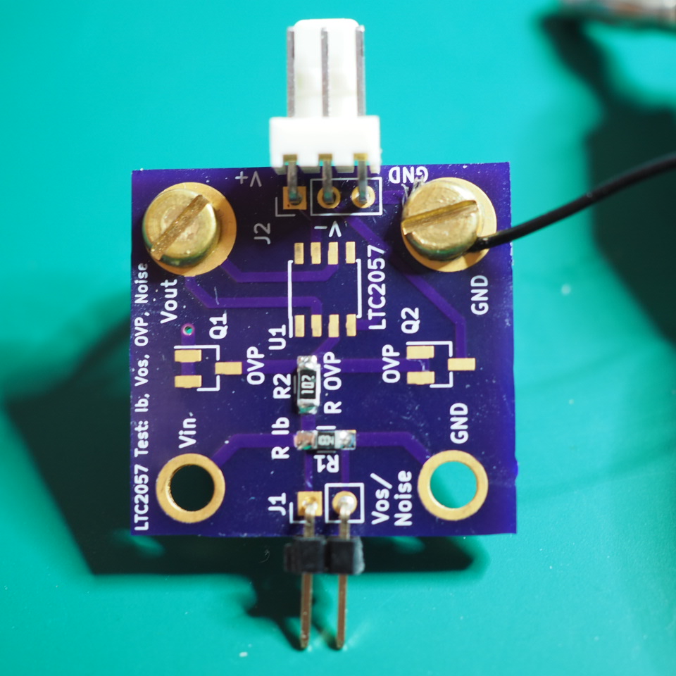
      To do these tests, I made a small PCB for above tests plus possibility to measure the leakage of over-voltage protection JFET. Later I realized that it is not the perfect PCB and the second version is already developed, but I have to wait for the end of the current world pandemic situation. In the first PCB version I forgot :
      • the bypass capacitors, so I have to solder them at the back of the PCB near to  the supply pins. Without them the results are really scrappy.
      • to add guard ring around the input positive terminal of the op-amp. This is a recommendation found in the datasheets for current leakage limitation. 
      • the possibility to disconnect the 1MOhms resistor from the ground that is required for the linearity test.  
      • the load resistor between the op-amp output and the ground.
      Additionally I added OVP with double diodes (for BV199) in SOT23 package, feedback resistor required for some op-amps. Here is the layout of the second PCB version:


      Other tests which can be made, but I do not have proper equipment or the time for that:
      - IBias vs. Vcm using Source Meter Unit. This characterization test can be seen in many datasheets. Unfortunately I do not have such equipment, therefore I can't make a test. I looked for low-cost solution and I found an evaluation board of AD5560 parametric measurement unit, but the lowest range was 5uV that required external 24 bit ADC to make pA measurements. The proper SMU like Keithley 236 is capable to measure down to pA range, but it is still in the 1300 - 2000 USD price range in EBey without shipping and VAT. 
      - Vos vs. Temp using thermo-regulated chamber.
      - Vos long term drift.

      Here are the pictures for the first version of the test PCB which I order from OSHPark. When op-amp is in the MSOP-8 package I solder it on the breakout board and PTFE cables are used to connect to the main test PCB: 


      Results from the tests

      First I made noise tests with short input and 1 MOhms resistor for the R6581 and HP 34401 as reference. The conditions were: 10V Range, Hi-Imp mode, AZero On, 100 NPLC, 50 samples.

      R6581HP 34401Keitley 2000Keitley 2002
      STDEV, uVP2P, uVSTDEV, uVP2P, uVSTDEV, uVP2P, uVSTDEV, uVP2P, uV
      Vnoise Zero0.06-0.1060.2-0.30.48-0.62-2.50.834-0.883.44-40.598-0.7342.92-3.37
      ENOD Zero8.3-8.058.08-7.97.4-7.37.08-6.987.16-7.136.8-6.777.56-7.477.17-7.11
      Vnoise 1M0.197-0.3471-2.70.514-0.7142.1-3.52.38-3.6410-201.58-1.9526.13-28.95
      ENOD 1M7.78-7.537.38-6.957.36-7.237.06-6.836.7-6.56.38-6.077.14-7.056.22-6.18

      I made more than 20 measurements with 50 samples each for the R6581 and HP 34401 and 2 measurements with 50 samples for the rest of the DMM. In the table it's shown the minimum and maximum values of the STDEV, peak to peak values in microvolts and respective ENOD values. You can see from the data, that R6581T and Keithley 2002 lost one digit when 1MOhms resistor was attached to the op-amp's input. On the other hand, the HP 34401A keeps very closely to the 7 digits even with input 1MOhms resistance: the average ENOD from 20+ measurements was 6.93.

      The next table shows the tests for the following parameters: Vos, Ibias, Linearity, Voltage RMS and peak to peak noise when inputs are shortened and when 1MOhms input resistor is used. 
      The first few bias current measurements of the MCP6V51 where far away from the specification limits (5.5nA bias current) so I decided to skip the rest of the tests. Because it was hard to solder and de-solder other MSOP-8 op-amps (I damage tracks on one of the test PCB) I skipped tests for the second MCP6V51 too. And decided to keep testing the third LTC2057HV which was in MSOP-8 package.

      Results with
      test board
      ver. 1
      Package
      Vos, uV
      Ib, pA
      min-
      max
      Ib, pA
      max spec
      Linearity,
      ppm
      Rout =
      open
      Linearity,
      ppm
      Rout=10K
      Noise, uV
      Zero, STDEVZero, p2p1M, STDEV1M, p2p
      LTC2057HV 1soic-83 - 653.66 - 62.192000.4911.2910.107 - 0.1590.4 - 0.71.257 - 1.975.73 - 9
      LTC2057HV 2soic-80.9 - 7.2688 - 7362000.4731.2140.113 - 0.2010.4 - 0.91.767 - 7.656.4 - 34.4
      LTC2057HV 3msop-85.4 - 712.9 - 33.5200N.A.N.A.0.117 - 0.2300.5 - 1.11.59 - 2.627.2 - 11.8
      ADA4522 1soic-8-0.2 - 0.31002.4 - 1004.71500.0550.0590.128 - 0.1180.4 - 0.61.63 - 5.446.7 - 30
      ADA4522 2soic-80.8 - 1.8692 - 6951500.10.0360.112 - 0.2430.6 - 0.83.26 - 10.715.8 - 43.8
      MCP6V51I 1msop-8-0.2 - -0.35502 - 5510250N.A.

      The only op-amp which passed the bias current tests was the third sample in msop-8 package. The first one was very close to the 50 pA limit. The second sample was 3-4 times above the specification limit. The rest of the op-amps failed as well.

      All LTC2057HV and ADA4522 passed the noise tests with 7 digits ENOD for short input test and 6 digits ENOD for 1MOhms input resistor.

      Linearity results were under 1ppm for LTC2057HV and ADA4522 when the output is not loaded, but when 10K load resistor is connected, the linearity cross the threshold of 1ppm for the LTC2057HV. Probably the reason is the missing sense connection from the op-amp output to the resistor and the voltage drop over the resistor leads can worse the linearity measurements. I already made correction in the test PCB ver.2 and if this does not help, I have to use a current buffer like in my LTZ1000 voltage reference to resolve this issue.

      Based on my initial tests, I can answer to my question in the beginning of this post: single buffer op-amp solution as front-end is feasible, but test of the buffer op-amp is required. Relaying only to typical or even maximum parameter's values in the datasheet is not enough.


      This post is still in progress. Once I get the test PCB ver. 2, I will buy more op-amps and will do a second try.

      Saturday, February 15, 2020

      Revised analog front-end : possible errors, part 1/4


      This is the beginning of a 4 part post about revising the analog front-end of the Voltmeter. It is based on gained calibration knowledge and the new collected information during the last 2 years:

      Part 1: Identifying possible errors in the analog front-end.
      Part 2: Selection and characterization of the input buffer op-amp. Here I will check if a single op-amp solution can be found with newer op-amps available in the market.
      Part 3: Over-voltage protection.
      Part 4: Replacing the analog switch in initial design with a shut-down feature of the LTC2057 op-amp.

      If a single input buffer op-amp solution can't be found in part 2, I will have to test the classical source follower, the common source differential amplifier and/or the bootstrap schematics. Eventually this will come as an additional 5th part.

      In 2016 year I started a research for the analog front-end of the voltmeter and now I'm in a process to make the first prototype. In the first posts at this time, I focused on over-voltage protection, dual polarity input handling and the automatic voltage range. I used a simulator/breadboard prototyping and looked for existing schematics in application notes or in the internet. I didn't really thought of the errors caused by the analog front end. So right now I'm going to  identify, analyze and test them.

      Why do they matter? Well, the measurement process is not only taking the measurement result from the DMM display, but also the calculation of uncertainty based on all data available in the DMM specification and the possible errors due unit under test characteristics.

      Most of the errors come from the resistance of the unit under test. Measuring a voltage source with high source resistance (like high value resistor dividers during calibration process) or high value resistance can be challenging for some existing DMM models. For this reason I will limit the maximum error to 10ppm when the source resistance is 1MOhms. This will be my criteria for the input buffer components selection. The limit will be 1ppm for errors that do not correlate with the source resistance.

      Just an example on why this matters: even if you want to calibrate the 1V range from 10V voltage standard using the Fluke 752A reference divider with output ratio uncertainty of 0.2ppm, there will be still a significant error from DMM bias current due to the high output resistance of the Fluke 752A. The output resistance is 40KOhm and if you are trying to calibrate the 1V range for a DMM with 10pA leakage current, it will create a parasitic voltage with a value of 0.4uV. And this value is 0.4 ppm regarding to the output which will be added in the final uncertainty.

      Firstly, let's try to identify the possible errors which can be found in the analog front end and the requirements that affect the specification. I'm aware for 8 of them so far: 

      • Thermal EMF.
      • Current leakage.
      • Loading error.
      • Long term and temperature drift of resistors used in the pre-amplifier.
      • DC amplifier's errors due to voltage offset, none-linearity, noise and common mode rejection ratio. 

      I'm interested only for those errors that affect the input buffer in the front of the ADC. I want to make an error budget which will allow me to select a preferable op-amp. 


      - Thermal EMF errors which affect low-level dc voltage measurements. They are caused by the connection of dissimilar metals at different temperatures. This can be happen when:
      • connections between the unit under test and the DMM PCB are made from different materials. Connections made by copper or silver wires and usage of low thermal EMF binding posts made by tellurium copper are preferable. Wire crimping between the binding posts and the DMM PCB is better than  wire soldering. 
      • electro-mechanical relays are used for high voltage ranges. In this case low EMF relay are preferable.

      - Errors caused by leakage currents
      When a high resistance circuit is measured, any current leakage will generate a parasitic voltage offset which will cause an error in the measurement process. The formula is V error = I leakage * R source. Origins of the leakage currents can be:
      • input bias current in the input buffer. This can be caused by JFET pair or op-amp, depends on schematics.
      • reverse leakage current in over-voltage clamping diodes.
      • contaminated PCB. This can be solved with PCB cleaning and active guarding.
      • cable leakage or leakage caused by binding posts insulation.
      I managed to collect information about the input bias current for several 6.5, 7.5 and 8.5 digits DMM and then made some real measurements with 10MOhs resistor connected to input binding posts. And here are results:

      6.5 Digits DMMInput Bias Current7.5 Digits DMMInput Bias Current
      TEK DMM4050 by datasheet<30 pAKeysight 34470A by datasheet<30 pA
      HP 34401A by datasheet<30 pAHP 34420A by datasheet<50 pA
      HP 34401A real measurement4-6 pATek DMM7510 by datasheet<50 pA
      Fluke 8845/6 by datasheet<30 pAKeithley 2001 by datasheet<100 pA
      Keysight 34465A by datasheet<30 pA8.5 Digits DMM
      Keithley 2000 by datasheet<100 pAHP 3458A by datasheet<20 pA
      Keithley 2000 real measurement4-8 pAFluke 8588A by datasheet-/+ 20pA
      Rigol DM3068 by datasheet<50 pAAdvantest R6581T real meas40-45 pA
      Rigol DM3068 real measurement40-45 pAFluke 8508A by datasheet<50 pA
      Siglent 3065x by datasheet<50 pAKeithley 2002 by datasheet<100 pA
      Siglent 3065x real measurement90 - 150 pAKeithley 2002 real measurement15-16 pA

      For the real measurements I used a small PCB with soldered 10MOhms resistor. Voltage range was set to 10V or 20V depends on DMM model, High impedance mode, highest possible NPLC value and all DMM were warm-up between 2 and 4 hours before taking the measurements.
      I tested 2 HP 34401, 2 Siglent 3065x, 2 Rigol DM3068, 1 Advantest R6581, 1 Keithley 2000 and 2002. Only both Siglent 3065x were out of the spec.


      The screenshots for Siglent DMM are taken from two different units. One of them had ~90-100pA leakage and the second one had ~140-150pA leakage.

      Limiting the error due leakage currents to less than 10ppm error, when input resistance is 1MOhs, means that my analog front-end must have less than 100pA current leakage. I will reserve 50pA for op-amp bias current, 30pA for clamp diodes and 20pA for the rest of the error origins.

      When ultra low-current or ultra-high resistance has to be measured, another type of measuring devices called "Electrometers" are used. They have fA range bias current and can measure giga-ohms resistors. Models from top-brand manufactures are: Keysight B2980A Series and Keithley 6514 / 6517B.

      - Loading error
      This error can be calculated with the following formula : R source / (R source + R dmm). Most of the bench DMM have at least 10GOhm input resistance, which guarantees less than 1ppm error when unit under test have less than 10KOhms resistance.
      Note that the common-mode input resistance is equal to the change in input bias current relative to the change in the buffer's input voltage  Some of the op-amp manufactures specified the minimum value of this parameter, but not all of them.

      For this error I will look for an op-amp which has at least 100GOhms input resistance. This will limit the error in the range of 10ppm if the source resistance is 1MOhms. 

      Errors due to resistors used in the pre-amplifier
      When the input voltage is significantly less than the native ADC range (10 or 20V), an DC amplifier is used to increase it. Resistors used in the amplifier suffer from temperature and long term drifting. They also can contribute to the error noise budget of the whole system if high values are selected. 

      - Errors due to input voltage offset of the op-amp
      • Vos drift due to temperature changes (Vos TC).
      • Vos long-term drift. Not all manufactures mention their long term drift of the Vos.
      These errors are almost eliminated in the zero drift op-amp, but these classes of op-amp usually suffer from higher current density noise.

      I would select maximum 1uV/C for Vos TC if none zero drift op-amp has to be selected.

      - Common Mode Rejection Ratio (CMRR)
      This parameter of the none inverting input buffer specify how well the op-amp will reject the parasitic signals from both the input and the ground. Most of the modern op-amp have CMRR value of at least 120dB which suppresses 1V input parasitic common mode voltage signal to 1uV output error (1ppm). For the 10ppm error, the CMRR has to be at least 100dB.
      The formula for the error caused by CMRR is:
      V out error = Vcm /(10-CMRR/20).
      Note that CMRR is decreasing while increasing the frequency of the input signal. CMRR is increasing proportionally with the op-amp gain.

      - Linearity error
      When an op-amp is used in unity gain mode, the none-linearity error is usually in the ppm and sub-ppm range. The none-linearity error is proportional to the gain and can be of a significant value if gains of 10 and 100 are used for 1V and 0.1V ranges.
      More information can be found in the following link.

      - Noise which affects the DMM resolution
      Noise level determine the maximum resolution of the DMM.
      The effective number of digits (ENOD) can be calculated by the following formula for 99.7% probability:
                 Digits = Log10( Full Scale Voltage Range/ Peak-Peak of the noise)

      The following noise sources caused by the input op-amp are:
      • input voltage noise
      • input current noise
      • thermal noise of the gain resistors in the DC amplifier
      For now I will skip the gain resistor noise and I will focus only on input voltage and current noise when high source resistance exists. The total sum of the RMS noise can be calculated with the root sum squared method:  

      Noise RMS = SQRT (VnoiseRMS2+(InoiseRMS*Rsrc)2+ Rsrc thermal noise RMS2)

      The RMS noise of 1MOhms resistor is 0.41uV for 10Hz frequency bandwidth.

      The peak to peak value can be estimated by multiplying by 6.6 the total RMS noise value. This will give us 99.9% confidence level.

      If the noise is given only with its spectral density, the RMS value is calculated with multiplication of the spectral density and square root of the desire bandwidth (10Hz). This is valid only when the noise is a flat curve between 0.1 and 10Hz.
      For example if the current spectral noise is 100fA/√Hz, the RMS value is 100fa * √ 10 Hz =  316.23 fA RMS. If the source resistance is 1MOhms, the RMS voltage noise will be 0.316 uV or 2.1 uV p2p. 

      When the source resistance is relatively low, the dominant will be the input voltage noise. High value of the source resistance multiplied by the input current noise can exceed the input voltage noise.

      Bellow are shown the noise limits for the op-amp buffer for different ENOD and voltage ranges:
      • 44uV p2p noise for 6 digits ENOD and 22 V range / 44V full scale
      • 4.4uV p2p noise for 7 digits ENOD and 22 V range / 44V full scale
      • 24uV p2p noise for 6 digits ENOD and 12 V range / 24V full scale
      • 2.4uV p2p noise for 7 digits ENOD and 12 V range / 24V full scale
      ADI tutorial for op-amp noise can be found the following link.
      An excellent explanation video in 4 parts about op-amp noise can be watched here.   

      I was able to find only two low level noise voltmeters, called also nano voltmeters: HP 34420 and Keithley 2182A . They both are 7.5 digits. For 1MOhs source resistance HP 34420 is specified to 90nV RMS noise and for Keithley 2182A the noise is 350 nV RMS.

      In the next post I'm going to select one from several op-amps depending on error budget and I'm going to perform some tests to check if real parameters are better than the datasheet.

      Here is the summary of my error budget for the input op-amp excluding the noise limitations, mention above:

      Errors due:Parameter valueError, ppmConditions
      Current leakageIb < 50pA< 5 ppm<1MOhms Rsrc, 10V Range
      LoadingRin > 100GOhms< 10 ppm<1MOhms Rsrc
      CMRR>-120dB< 1 ppm
      Linearity< 1 ppmUnity gain
      Vos TC< 1uV / C< 0.1 ppm10V Range

      Update : a friend of mine send me a article from EDN : Design femtoampere circuits with low leakage. I think it is worth to add a link here: part 1, part 2 and part 3.

      Tuesday, December 31, 2019

      Happy new 2020 Year!

      I would like to thanks to all visitors of this blog! Every your visit or e-mail from you makes me more motivated. This year I had visitors from 60 countries and 270 towns across the world with around 400 page views per month.  


      This year was busy for me and I do not had enough time to update the blog content. So this post will be summary what I achieved in 2019 year.

      Let's starts with latest new : last week I made a new workbench. Previously I used an old 0.5 sq. m. desk for work and one small table for making measurements. The space was limited and I decided to "upgrade" the workbench. The new one have more than 4 sq. m. unfolded area. Now I have plenty space and reserved some for next instruments which I have plan to buy in the next years.

      The second news is that I'm working on the first PCB prototype of the voltmeter. If everything is according the plan, it should be available in March next year. 

      The third news is related to my sub-project : high resolution (0.001°C) and accuracy (< 0.01°C per year with 25 ppm reference resistor) thermometer based on ADS 122U04 IC. I already made a prototype (available here) and the final PCB arrived and waiting to be solder. The software is also in the final stage. I still waiting the Gallium which is needed for calibration of the thermometer. I made also a "Gallium Melting-Point Standard" from PTFE to hold the Gallium. This will allow me to calibrate the thermometer in the range of 0°C to 29.76°C with uncertainty less than 0.015°C if the Ga which I bought have at least 99.99% purity.


      The last news is related to the feature of this blog. In the 2018 after buying my first 6.5 and 8.5 digits DMMs, I thought how to secure my project financially. For the HP 34401A I made several short PCBs for measuring the noise and zero offset. Unused PCB I listed in Ebay and I was surprised how quick they sold out. So this year the profit from Ebay sells was enough to cover my 4 calibrations in National Institute of Metrology. If I have enough sells during the next 2020 year I think to make an open HW/SW company (www.seidocmt.eu) which sells will allow me to continue to work on this open source project.

      Also, you can follow me on twitter : @CmtSeido.